December 12th
Cutting Edge Technologies of Power Semiconductor Device Applications for Electric Vehicle’s Power Electronics Systems in Japan, US, Europe and China Case
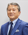
Prof. Masayoshi Yamamoto
Professor,
Institute of Materials and Systems for Sustainability (IMaSS),
Graduate School of Engineering and School of Engineering,
Department of Electrical Engineering,
Nagoya University
Abstract
The Electric Vehicle’s power electronics systems have required the advanced technology for obtaining high power density and high performance in power semiconductor device applications. In this presentation, the demand technique for EV will be discussed using teardown report of Model 3 (TESLA), Mustang Mach-E (Ford), ID.3 (VW), Taycan (Porsche) and HongGuang Mini EV (Wuling).
Furthermore, the possibility of SiC and GaN power semiconductor applications for EV will be discussed from the experimental point of views in case of the main inverter, 3-phase inverter for the compressors, the on-board charger and the isolated DC-DC converter.
CV
Masayoshi Yamamoto (M’11) received his M.S. and Ph.D. degree in science and engineering from Yamaguchi University, Yamaguchi, Japan in 2000 and 2004 respectively. From 2004 to 2005, he was with Sanken Electric Co., Ltd., Saitama, Japan. From 2006 to 2017, he was with the Interdisciplinary Faculty of Science and Engineering in Shimane University, Japan, as an Associate Professor. He is currently a Professor at Institute of Materials and Systems for Sustainability (IMaSS), Nagoya University, Japan. His research interests include power supply for HEV (boost converter, buck converter, 3-phase inverter, digital control), charging system for EV, LED illumination system for a tunnel, EMI of switching power supply, and wireless power transfer.
The Contribution and Expectation of TSMC Japan 3DIC R&D Center to Japan Industry
Only live presentations are available. No Q&A.
No recordings or on-demand.
Mr. Yutaka Emoto
Vice President,
TSMC Japan 3DIC R&D Center, Inc.
Abstract
Connecting Our Japanese Partners to Our Worldwide Customers by Material Development in 3D IC
With the advent of 3D IC and associated packaging technology, semiconductor industry has focused not only on SoC scaling to follow Moore’s Law, but also concurrently focused on chiplet integration through 2.5D and 3D stacking technologies to increase circuit densities as alternative approaches to catch up with classic Moore’s Law and intended to further extend Moore’s Law through innovative chiplet integration evolutions. In TSMC, advanced 3DFabric platforms, CoWoS family and INFO family, have been developed and widely adopted by global semiconductor industry.
TSMC established its Japan 3DIC R&D Center subsidiary in March 2021 and completed the clean room construction this June. TSMC Japan 3DIC R&D Center will support research and development of state-of-the-art 3D IC packaging material. Connecting our Japanese partners possessing strengths in semiconductor materials, substrate, and equipment, to TSMC’s worldwide customers, we look forward to creating a new market of 3D Fabric and 3D IC and contributing to semiconductor industry in Japan.
CV
Emoto started his career at Hitachi Ltd and Renesas Electronics, where he was responsible for Corporate planning, Sales and Marketing and Global procurement.
After joining J-Devices in 2018, he led the company as the President and Representative Director during the economy recession period.
He joined TSMC in 2021 to establish Japan 3DIC R&D Center and successfully moving forward to the R&D business activities after the Opening Ceremony in June.
Emoto Graduated from the University of KEIO with a degree in Engineering.
December 13th
The Path to 100 Billion Goes Upward – IBM Research Semiconductors Technology Atlas
Dr. Nelson Felix
Director, Process Technology
IBM
Abstract
Recently, IBM Research published a Research Technology Atlas (https://research.ibm.com/roadmap/), a collection of interconnected roadmaps across the research portfolio. During this talk, we will discuss our strategic goals for the next three years regarding semiconductor research, which suggests the main scaling paths are starting to look upward, from stacked FETs to advanced chiplet technology. Key gaps and research focus areas will be highlighted: a rallying cry for the industry as well as our partners on the challenges and opportunities for the future.
CV
Nelson Felix joined IBM in 2008 and is currently the Director of Process Technology at IBM Research in Albany, NY. In this role, Nelson is responsible for the demonstration and enablement of new tooling, processes, materials, and metrology to support IBM’s leading-edge CMOS device and AI hardware roadmap. Nelson received his B.S. from the University of Massachusetts, Amherst (2002) and his Ph.D. from Cornell University (2007), both in chemical engineering, and his doctoral work centered on the characterization of novel photoresist materials for EUV. Dr. Felix is an SPIE Fellow, and he is co-inventor on over 50 patents and co-author on over 100 publications.
A Requirements Driven Digital Twin Framework to Support Semiconductor Manufacturing: Specifications and Opportunities
Dr. James Moyne
Dr. James Moyne, Ph. D.
Associate Research Scientist, Mechanical Engineering Department
University of Michigan
Consultant for Standards and Technology, Advanced Services Engineering , Applied Global Services, Applied Materials
Abstract
Among the tenets of Industry 4.0 or Smart Manufacturing (SM), digital twin (DT), which represents the capabilities of virtual representations of components and systems, has been cited as the biggest technology trend disrupting engineering today. DT concepts have been in use for years in semiconductor manufacturing in analysis and control areas such as model-based process control (i.e., “Run-to-Run Control”), predictive maintenance, and virtual metrology. Moving forward a framework is needed that will support the expected pervasiveness of DT technology in the evolution of SM. This framework must promote solution re-usability, interoperability, interchangeability, maintainability and extensibility, within and across analysis and control solution areas. It must support the entire DT lifecycle process including creation, verification and validation, deployment, and maintenance. Most importantly the framework should allow for information sharing in a pre-competitive and secure competitive spaces. In this presentation, background on the current state of the DT space in semiconductor manufacturing will be provided. A requirements driven DT framework will then be described that can support the evolution of existing DTs and allow for advancement in the DT space to support SM objectives. Examples will be provided illustrating the use of the framework to support re-usability and extensibility of analysis and control solutions.
CV
Dr. James Moyne is an Associate Research Scientist at the University of Michigan, where he received his Ph.D. degree. He is also a consultant for standards and technology to the Applied Global Services group at Applied Materials working in microelectronics and pharmaceutical industries. Dr. Moyne has over 25 years of experience in semiconductor manufacturing process automation and control including starting and running the first company that provided run-to-run (R2R) control solutions for semiconductor manufacturing. His focus area over the past 10 years has been in smart manufacturing topics including digital twins, prediction technology (predictive maintenance, virtual metrology, and yield prediction), and analytics. He is the author of a number of refereed publications, holds patents in each of these areas, and is co-author of the book Run-to-Run Control in Semiconductor Manufacturing. He currently co-chairs the Factory Integration Thrust of the International Roadmap for Devices and Systems (IRDS), and the SEMI Information and Control Committee.
Heterogeneous Integration Paving the way for Microelectronics Resurgence
Mr. Timothy Lee
IEEE Board of Director
IEEE HIR Chair for 5G Technical Working Group
Abstract
Heterogeneous Integration through packaging innovations is widely acknowledged as being increasingly important to drive performance, system availability, power efficiency, cost and time to market of microelectronics systems, from High Performance Computing & Data Centers, to 5G & beyond, Mobile, Autonomous automotive, Internet of Things, Medical and Health Wearables. We are at a unique point in time when there is a global recognition on the critical roles of semiconductor and microelectronics as foundational pillars to nations’ economies. There is immense need for the Heterogeneous Integration technology roadmap addressing an Ecosystem Agenda comprising of future vision, difficult challenges and potential solutions to pave the way for Microelectronics Resurgence.
CV
Timothy Lee, currently a Boeing Technical Fellow, is responsible for the development of RF and digital electronics for advanced communications networks and sensor systems, AI/ML applications and edge processing at The Boeing Company (1998- Present). He is leading the development of state- of- the- art hardware which are based on CMOS/SiGe, GaAs, InP and GaN integrated circuits and devices. Current interests include techniques to overcome the End of Moore’s Law which includes novel semiconductor device technologies, 2.5D/3D heterogeneous integration, hardware designs for 5G millimeter- wave systems and trusted microelectronics. He has 40 years of professional experience with broad technical and managerial responsibilities.
He is an active volunteer in the IEEE, having served multiple roles across Technical Activities and Member Geographic Activities. His most recent roles are:
- Member of the IEEE Board of Directors
- Director of IEEE Region 6 (Western US)
- Member of IEEE Industrial Engagement Committee
- Member of IEEE New Initiative Committee
- Co-Chair of IEEE Future Networks Initiative
- IEEE Heterogenous Integration Roadmap
- Co-Chair of Aerospace & Defense TWG
- Co-Chair of the 5G / mm-waves TWG
- President of IEEE Microwave Theory and Technology Society (2015)
Decarbonization Management to Improve Corporate Value
Mr. Michitaka Tokeiji
Founder and CEO, Zeroboard. Inc
Abstract
In the global decarbonization trend, companies are required to calculate and disclose not only the CO2 emissions from the energy they use (Scope 1 and 2 in the GHG Protocol), but also the emissions of their entire supply chain.
Scope 3 is the amount of CO2 emissions from supply chains other than the company’s own activities. For example, how much CO2 is emitted by the providers of goods and services procured in the course of corporate activities (Scope 3 upstream) and how much CO2 is emitted by the goods and services sold by the company (Scope 3 downstream).
In this presentation, we will explain the intention behind the disclosure of CO2 emissions, including Scope 3, and its impact on the entire supply chain, so that it can be used for strategic planning for decarbonization management.
CV
Tokeiji started his career at JPMorgan and then moved to Mitsui and Co. Ltd., where he was involved in energy-related venture investment and new business development in the ICT Business Division. After joining A.L.I. Technologies in 2018, he led the Software Business Department and started the development of the cloud service for GHG emission calculation and visualization. In 2021, he did an MBO of the business and founded Zeroboard Inc. Tokeiji graduated from the University of Tokyo with a degree in Engineering.


